


Schedule a Call Back
Delhi Institutions Support India Semiconductor Mission
2026-03-11
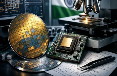 The Government of India has prioritised talent development through training, upskilling and workforce development under the Chips to Startups initiative of the India Semiconductor Mission, with officials noting progress in four years towards a 10-year target of training 85,000 engineers in semiconductor design. Electronic design automation tools provided by Synopsys, Cadence, Siemens, Renesas, Ansys and AMD have been deployed in 315 academic institutions, enabling students to gain practical chip design experience. Chips have been fabricated and tested at the Semiconductor Laboratory, Mohali, and the programme has become the world's largest open-access EDA programme with 18.5 million hours (mn hours) of tool usage to date.
Students from universities across the nation are participating in semiconductor design and related disciplines, and under Semicon 2.0 the programme will be expanded from 315 universities to 500 universities to create a strong base of skilled engineers. The initiative seeks to integrate academic curricula with industry standard tools and laboratory facilities to strengthen employability and practical competence. Officials indicated that expanding access to EDA tools will widen participation and accelerate skills development in multiple regions.
As the global semiconductor industry reaches USD two trillion (tn), officials estimate nearly two million (mn) skilled professionals will be required, offering substantial employment opportunities. Major National Capital Region institutions supporting training and validation include Indian Institute of Technology Delhi, National Institute of Technology Delhi, Indraprastha Institute of Information Technology Delhi, Delhi Technological University, Netaji Subhas University of Technology, Jawaharlal Nehru University, Indira Gandhi Delhi Technical University for Women, Vivekananda Institute of Professional Studies and DV2JS Innovation LLP.
Advanced EDA tools and enhanced training infrastructure are enabling students to design functional chips and gain validation and testing experience, thereby strengthening the national semiconductor talent base. The Government has emphasised that Semicon 2.0 will continue to promote design, manufacturing and innovation to establish India as a global hub, supported by sustained investment in training and industry collaboration.


Subscribe Now
Subscribe to our Newsletter & Stay updated
RECENT POSTS
Popular Tags
Folliow us